
TMS320VC5509使用nof flash AM29LV400
Flash 使用
2023-09-14 08:57:21 时间
1. 硬件接口如下,其中nor flash的使用方法,写的时候和NAND FLASH是一样的,读的时候和DRAM是一样的

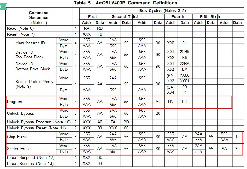
2. 看下擦除指令和编程指令
3. 代码如下
#include <csl.h>
#include <csl_pll.h>
#include <csl_emif.h>
#include <csl_chip.h>
#include <stdio.h>
#include <csl_gpio.h>

//#define AM29_FLASH_ADDR_BEGIN   (*((unsigned int *)0x200000))
#define AM29_FLASH_ADDR_BEGIN   ((unsigned int *)0x200000)
#define DATA_BUF_LEN 20
/*锁相环的设置*/
PLL_Config  myConfig      = {
  0,    //IAI: the PLL locks using the same process that was underway
                //before the idle mode was entered
  1,    //IOB: If the PLL indicates a break in the phase lock,
                //it switches to its bypass mode and restarts the PLL phase-locking
                //sequence
  6,    //PLL multiply value; multiply 12 times
  12             //Divide by 2 PLL divide value; it can be either PLL divide value
                //(when PLL is enabled), or Bypass-mode divide value
                //(PLL in bypass mode, if PLL multiply value is set to 1)
};
/*SDRAM的EMIF设置*/
EMIF_Config emiffig = {
  0x221,     //EGCR  : the MEMFREQ = 00,the clock for the memory is equal to cpu frequence
              //          the WPE = 0 ,forbiden the writing posting when we debug the EMIF
              //        the MEMCEN = 1,the memory clock is reflected on the CLKMEM pin
              //        the NOHOLD = 1,HOLD requests are not recognized by the EMIF
  0xFFFF,    //EMI_RST: any write to this register resets the EMIF state machine
  0x3FFF,    //CE0_1:  CE0 space control register 1
              //        MTYPE = 011,Synchronous DRAM(SDRAM),16-bit data bus width
  0xFFFF,   //CE0_2:  CE0 space control register 2
  0x00FF,   //CE0_3:  CE0 space control register 3
              //        TIMEOUT = 0xFF;
  0x1FFF,    //CE1_1:  CE0 space control register 1
            //        Asynchronous, 16Bit
  0xFFFF,    //CE1_2:  CE0 space control register 2
  0x00FF,    //CE1_3:  CE0 space control register 3
  0x1FFF,    //CE2_1:  CE0 space control register 1
            //        Asynchronous, 16Bit
  0xFFFF,    //CE2_2:  CE0 space control register 2
  0x00FF,    //CE2_3:  CE0 space control register 3

  0x1FFF,    //CE3_1:  CE0 space control register 1
  0xFFFF,    //CE3_2:  CE0 space control register 2
  0x00FF,    //CE3_3:  CE0 space control register 3

  0x2911,   //SDC1:   SDRAM control register 1
              //          TRC = 8
              //        SDSIZE = 0;SDWID = 0
              //        RFEN = 1
              //        TRCD = 2
              //        TRP  = 2
  0x0410,    //SDPER : SDRAM period register
              //          7ns *4096
  0x07FF,    //SDINIT: SDRAM initialization register
              //        any write to this register to init the all CE spaces,
              //        do it after hardware reset or power up the C55x device
  0x0131    //SDC2:      SDRAM control register 2
              //        SDACC = 0;
              //        TMRD = 01;
              //        TRAS = 0101;
              //        TACTV2ACTV = 0001;
  };


void  delay(unsigned int d_time)
{
    unsigned int loop = 0;
    while(d_time--)
    {
    loop = 1000;
    while(loop--);
    }
}

Uint16    ChipErase(void)
{
    Uint16    i,Data;
    Uint32    TimeOut;
    *(AM29_FLASH_ADDR_BEGIN + 0x555) = 0xAA;
    *(AM29_FLASH_ADDR_BEGIN + 0x2AA) = 0x55;
    *(AM29_FLASH_ADDR_BEGIN + 0x555) = 0x80;
    *(AM29_FLASH_ADDR_BEGIN + 0x555) = 0xAA;
    *(AM29_FLASH_ADDR_BEGIN + 0x2AA) = 0x55;
    *(AM29_FLASH_ADDR_BEGIN + 0x555) = 0x10;
    i = 0;
    TimeOut = 0;
    delay(8000);
    while(i<5)
    {
        Data = *(AM29_FLASH_ADDR_BEGIN +  0x1FF);
        if    (Data == 0xFFFF)    i++;
        else    i=0;
        if ( ++TimeOut>0x1000000)    return (0);
    }
    for    (i=0;i<0x400;i++)
    {
        Data = *(AM29_FLASH_ADDR_BEGIN + i);
        if (Data !=0xFFFF)    return (0);
    }

    return  (1);

}

Uint16    FlashWrite(Uint32    RomStart, Uint16*   buf_start,  Uint16    Length)
{
    Uint32    i,TimeOut;
    Uint16    Data1,Data2,j;
    for    (i=0;i<Length;i++)
        {
            *(AM29_FLASH_ADDR_BEGIN + 0x555)= 0xAA;
            *(AM29_FLASH_ADDR_BEGIN + 0x2AA)= 0x55;
            *(AM29_FLASH_ADDR_BEGIN + 0x555) = 0xA0;
            *(AM29_FLASH_ADDR_BEGIN + RomStart + i) = *(buf_start++);
            TimeOut = 0;
            j=0;
            delay(10);
        }

        while(j<5)
            {
                Data1 = *(AM29_FLASH_ADDR_BEGIN + RomStart + i);
                Data2 = *(AM29_FLASH_ADDR_BEGIN + RomStart + i);
                if    (Data1 == Data2)    j++;
                else    j=0;
                if ( ++TimeOut>0x1000000)    return (0);
            }
    return  (1);
}

void    FlashRead(Uint32    RomStart, Uint16*   buf_start,    Uint16    Length)
        {
            Uint32    i;

            for    (i=0;i<Length;i++)
                {
                    *(buf_start++) =  (*((volatile    unsigned  int  *)(AM29_FLASH_ADDR_BEGIN + RomStart + i)));

                }
        }

main()
{
    Uint16 data_buf[DATA_BUF_LEN] = {0};
    unsigned int i = 0;
    Uint16 write_buf[DATA_BUF_LEN] = {0x0001,0x0002,0x0003,0x0004,0x0005,0x0006,0x0007,0x0008,0x0009,0x0000,
                                      0x0011,0x0012,0x0013,0x0014,0x0015,0x0016,0x0017,0x0018,0x0019,0x0010};
    unsigned int test_data = 0;
    /*初始化CSL库*/
    CSL_init();

    /*EMIF为全EMIF接口*/
    CHIP_RSET(XBSR,0x0a01);

    /*设置系统的运行速度为144MHz*/
    PLL_config(&myConfig);

    /*初始化DSP的EMIF*/
    EMIF_config(&emiffig);
    /*确定方向为输出*/
    GPIO_RSET(IODIR,0xFF);
    GPIO_RSET(IODATA,0x00);
    ChipErase();
    FlashWrite(0, write_buf,  DATA_BUF_LEN);
    delay(1000);
    FlashRead(0, data_buf,  DATA_BUF_LEN);

    for(i=0;i<DATA_BUF_LEN;i++)
    {
        if(write_buf[i] != data_buf[i])
        {
            printf("test data error:%d",i);
        }
    }
    if(i == DATA_BUF_LEN)
    {
        printf("test data ok");
    }

    for(;;);
}
相关文章
- 创龙OMAPL138的SPI FLASH读写
- 如何用迅雷下载在网页中的Flash动画或课件
- 如何使用FLASHGOT下载网页FLASH
- Nor Flash的CFI与JEDEC接口
- 将海康大华等网络摄像机RTSP流进行网页Flash rtmp和H5 hls直播的技术方案
- EasyRTMP手机直播推送rtmp流flash无法正常播放问题
- 【不是问题的问题】为什么STM32的Flash地址要设置到0x08000000
- 【STM32H7】第21章 ThreadX GUIX外置主题,字库和图库到外部SPI Flash
- 【STM32F429开发板用户手册】第10章 STM32F429的FLASH,RAM和栈使用情况(map和htm文件)
- 【STM32F407开发板用户手册】第10章 STM32F407的FLASH,RAM和栈使用情况(map和htm文件)
- open-flash-chart2各种效果
- [闪存2.1.1] 固态硬盘存储介质闪存_闪存的物理结构_NAND_Flash工作原理
- SPI-Flash页写实验
- 图片本地预览 flash html5
- Ubuntu 14.04 下手动安装Firefox的Flash插件
- 【案例分享】基于CANoe的诊断Coding及Flash实现
- 使用NB Exploit Kit攻击的APT样本分析——直接看流程图,就是网页挂马,利用java和flash等漏洞来在你主机安装和运行恶意软件
- allegro制作通孔焊盘封装-flash热风焊盘-图文并茂的Allegro 通孔焊盘制作教程
- [闪存2.1.5] NAND FLASH基本读操作及原理_NAND FLASH Read Operation源码实现
- 基于SPI协议的Flash全擦除
- SPI FLASH的读写